
PCB manufacturing is a complicated technological process that requires appropriate production files. Depending on the program in which you design your files, their files extensions have different names. Files for the production of PCBs are GERBER. They define specific layers in the physical design of the PCB, and each file corresponds to one of them. However, in order to define drilling holes or milling parameters, the preferred format is Excellon.
| Extension | Layer |
|---|---|
| DRL lub TXT | Drill |
| GTO | Top Overlay (Silkscreen) |
| GTS | Top Soldermask |
| GBS | Bottom Soldermask |
| GTL | Top Layer |
| GBL | Bottom Layer |
| BRD | Board |
| GKO | Keep Out Layer |
| GTP | Top Paste |
| GBP | Bottom Paste |
| GPT | Top Pad Master |
| GPB | Bottom Pad Master |
| PHO | Photoplotter |
| RPT | Report |
| GMx | Mechanical Layer X (x corresponds to the layer number) |
| GPx | Inner Plane Layer X (x corresponds to the layer number) |
Important tips that shall facilitate and improve the manufacturing process:
1. please complete the PCB production valuation form carefully (here’s the link);
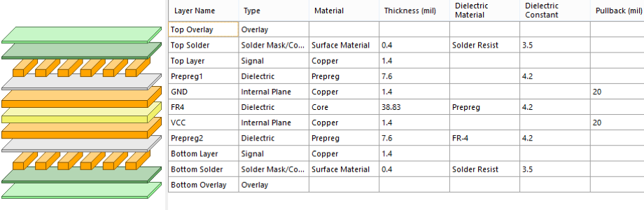
2. please make a stakcup (stretches of PCB layers) in a descriptive form, e.g. txt file or graphic or on a mechanical layer, and describe the layers with the appropriate names of production files;
3. please create a board outline / milling layer on a separate layer. Be sure to keep the right distance between the copper & milling line and the edge of the board so that it does not get damaged. Ideally, during the design process, add the Keep Out layer to help maintain the required distance;
4. when the impedance control is required, please create the appropriate table or description of requirements;
5. please optimize the number of defined diameter of holes and drillings, which reduce production costs. Holes should be marked accordingly as metallized (PTH) and non-metallized (NPTH). In the case of buried or blind vias, separate drilling files should also be made for their range in the stackup (from which to which layers it applies, which layers it connects) and describe them accordingly. Please specify the tolerance as well;
6. please create silkscreen/ overlay in a way that they do not overlap the pads - such descriptions will be cut in the production process;
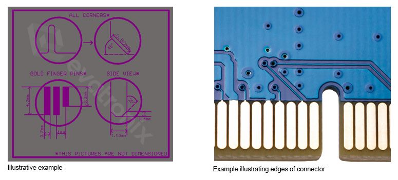
7. if the connector edges must have the appropriate dimensions and tolerances, please create an illustrative drawing as presented below:
If you have any problem with generating/creating production files, please contact us. Our technical department will be pleased to answer all your questions and help you erase any doubts.